IBM Reveals Quantum Chip Production Using Advanced 300mm Semiconductor Fabrication
November 13, 2025 · 3 min read
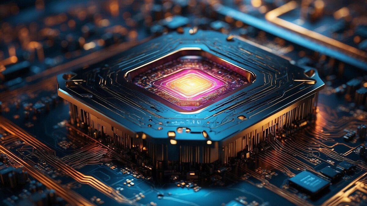
IBM has unveiled its quantum computing manufacturing breakthrough, revealing that current and future quantum processors are being fabricated using advanced 300mm semiconductor wafer technology at the Albany NanoTech Complex. This marks a significant shift from research-scale production to industrial manufacturing for quantum hardware.
The quantum computing race just got a manufacturing upgrade. IBM is now processing its IBM Quantum Loon and Nighthawk chips—along with all future processors on its development roadmap—using the same 300mm wafer technology that produces cutting-edge classical computer chips. This transition from specialized 200mm research fabrication to production-scale 300mm manufacturing represents quantum computing's maturation from laboratory experiment to industrial technology.
At the heart of this transformation is IBM's partnership with NY CREATES' Albany NanoTech Complex, one of the world's most advanced semiconductor research and development facilities. The public-private partnership, which began in 2002 with IBM, Tokyo Electron, and New York State, has evolved into a $20 billion semiconductor ecosystem. Now, this infrastructure is being leveraged to solve quantum computing's manufacturing challenges.
Christy Tyberg, IBM's Distinguished Engineer of Quantum Fab Technology Infrastructure, explained the strategic advantage: "If we had started processing our chips using 300mm technology, we wouldn't have achieved the success required to pull off our development roadmap." The shift enables 24/7 wafer processing with state-of-the-art automation while maintaining the flexibility of 200mm technology for custom research and development steps.
The manufacturing process begins with silicon wafers processed through automated systems that etch, deposit metals, and treat the surfaces to create rectangular grids of quantum chips. Unlike classical transistors measured in nanometers, quantum bits (qubits) require entirely different materials, wiring configurations, and fabrication approaches. The team had to develop new processes from scratch to achieve millisecond coherence times—the critical metric for quantum bit stability.
Hemanth Jagannathan, Distinguished Engineer and Director responsible for Process Technology R&D and Semiconductor Acceleration for Quantum at IBM Research, leads the semiconductor integration effort. "We became the accelerator for IBM's quantum hardware mission and roadmap," he stated. "There were needs articulated by the quantum team and we would understand them, figure out the processes involved, and how to build the devices with speed and scale."
The collaboration between quantum physicists at IBM's Thomas J. Watson Research Center in Yorktown and semiconductor experts in Albany has created a tightly coupled development process. Physicists design quantum chips capable of delivering the scale and performance required, while fabrication engineers translate these designs into repeatable manufacturing processes. The 300mm technology allows researchers to explore more chip designs in significantly less time, accelerating the innovation cycle.
With quantum processors like Heron, Nighthawk, and Loon already in production, and future chips including Kookaburra, Cockatoo, Starling, and Blue Jay on the horizon, IBM's quantum manufacturing capability positions the company uniquely in the race toward fault-tolerant quantum computing by 2029. As Jagannathan confidently stated: "We are probably the company on the planet that can do this."